
As OLED and MicroLED technologies race to deliver thinner, brighter, and more energy-efficient displays, one enabling innovation is helping these next-generation displays reach their full potential: microlens arrays (MLAs).
These microscopic optical components are essential to improving light extraction efficiency, boosting brightness, and reducing power consumption, all without increasing device size. And thanks to advances in high refractive index (HRI) materials and inkjet printing, MLAs are now not only high-performance but also scalable for mass production.
Why Microlens Arrays Matter in Display Technology
OLED and MicroLED displays offer exceptional image quality, deep contrast, and thin form factors, but they often suffer from light extraction inefficiency. A large portion of light generated by the display’s emissive layer gets trapped due to internal reflections and substrate limitations.
Microlens arrays address this challenge. By redirecting light that would otherwise be lost, MLAs significantly improve optical efficiency. For OLED and MicroLED devices, this translates into:
- Higher brightness without added power consumption
- Improved battery life in portable electronics
- Sharper, more uniform visuals across the display
To scale MLA technology for consumer electronics, however, manufacturers need a solution that is precise, repeatable, and compatible with high-volume production. That’s where inkjet printing and Pixelligent come in.
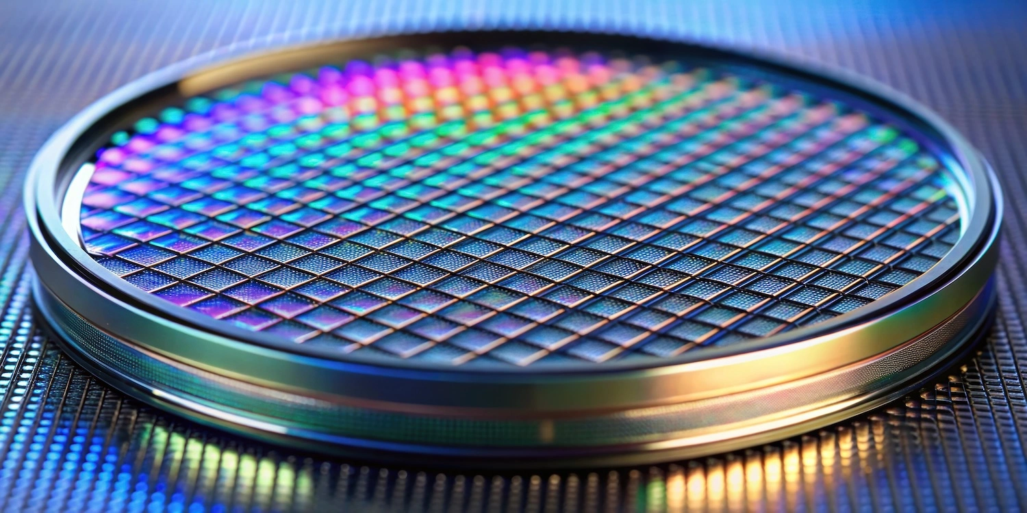
How Microlens Arrays Are Made for OLED & MicroLED Displays
Step 1: Nanocrystal Synthesis and Surface Modification
Manufacturing begins with the synthesis of nanocrystals – a small crystal structure composed of atoms or molecules arranged in a well-defined lattice. These nanocrystals must be uniform in size and shape to ensure predictable optical behavior.
Pixelligent enhances this process through surface modification. Using custom-designed capping agents, our nanocrystals are treated to improve their stability and dispersion in resin systems. This step is crucial for downstream inkjet printing performance and long-term material reliability.
Step 2: Formulation of High-Refractive Index Inkjet Materials
Once surface-modified, the nanocrystals are dispersed into monomers to create PixClear® formulations. These high refractive index materials (RI > 1.7) maintain:
- Excellent transparency
- Low haze
- Compatibility with standard inkjet printheads
The formulation’s surface tension is engineered to work with industry-standard inkjet tools, enabling precision deposition of microlens features at scale. This makes it possible to pattern MLAs directly onto OLED and MicroLED substrates using non-contact methods.
Step 3: MLA Fabrication via Inkjetting
The inkjet process enables digital, maskless printing of microlens arrays, offering significant advantages in cost, speed, and pattern flexibility.
The process typically includes:
- Inkjet deposition of the PixClear® formulation onto a display-compatible substrate in an arrayed pattern
- Template stamping or surface tension control to shape each droplet into a microlens dome
- UV curing to lock in lens geometry and provide mechanical and environmental stability
Key material performance criteria include:
- High refractive index for enhanced light redirection
- Defined contact angle and controlled surface energy for precise lens shape
- UV and thermal stability to withstand downstream processing and end-use conditions
- Inkjet processability for manufacturability at scale
Pixelligent’s materials are specifically designed to meet these challenges, resulting in repeatable, optically accurate microlens arrays optimized for OLED and MicroLED displays.
Pixelligent’s Role in Enabling Inkjet MLAs
Pixelligent is the industry leader in high refractive index nanocomposites, and our materials are powering the next generation of MLA-enabled displays. Our PixClear® process is uniquely suited to the demands of OLED and MicroLED inkjet applications.
Key benefits:
- Refractive index >1.7 for maximum light extraction
- High transparency and stability across printed microlenses
- Engineered for inkjet: Low viscosity, stable jetting, and excellent droplet control
- Proven reliability under UV and thermal stress
- Scalable for volume production, enabling cost-effective deployment across consumer electronics
Our partnership with Kateeva, a global leader in inkjet OLED equipment, reinforces our commitment to commercial-scale manufacturing. By integrating PixClear® formulations into their MLA printing platforms, we are helping manufacturers bring brighter, more energy-efficient OLED and MicroLED displays to market faster.
Trends Driving MLA Adoption in OLED and MicroLED Displays
The integration of MLAs into emissive displays provides a competitive advantage. As smartphones, AR glasses, and wearables continue to shrink in size, they demand compact optical components with tight performance tolerances. At the same time, display manufacturers are pushing for higher brightness levels in OLED and MicroLED panels. Improved light extraction achieved through MLAs also reduces the demand for higher driving voltages, enhancing power efficiency and supporting broader sustainability goals.
Additionally, the use of inkjet tools provides a flexible, cost-effective method for printing microlens patterns directly onto display substrates, accommodating rapid design changes and high-volume production needs. This flexibility is crucial in the fast-paced consumer electronics market.
The Future Is Bright – and Efficient
Inkjet fabrication, powered by advanced HRI materials, is the key to delivering this capability at commercial scale. Pixelligent’s PixJet®materials are making it possible. With unmatched refractive index, inkjet compatibility, and industry partnerships, we’re helping shape the displays of tomorrow.
Interested in enhancing your next-gen display applications? Contact Pixelligent to explore how our PixClear® materials can support your MLA strategy.